en
The Surface quality of optical parts is also called surface defects of optical parts. In the national standard GB/T 1185-2006, it is defined as: pitting, spots, scratches, broken edges and other defects on the surface of optical parts. In the process of actual production inspection, the inspection and maintenance of surface defects of optical parts is the most basic operation.
GB/T 1185-74
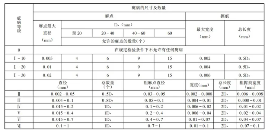
For the inspection standards of optical parts surface defects, the domestic optical industry has undergone several periods of development. Standard GB/T 1185-74 is the early domestic
optical processing industry generally adopted evaluation standards. The standard is divided into 10 levels according to the size and number of allowable defects on the surface of
optical parts. Classes 0 to I-30 apply to optical parts located on or near the image plane of the optical system, and II to VII apply to optical parts not located on the image plane of the
optical system. The main size and quantity requirements are shown below.
This standard has been used for 20 years, and even more optical processing and lens assembly manufacturers will still use this standard for evaluation. During this period, inspectors were mainly relied on to observe under an incandescent lamp of about 60w, and the background of the detection was black to make it easier to observe the defects of the parts, but this method was mostly suitable for transmitted light inspection. Defects that can be observed under partial reflected light are not easy to be found, and need to be found by relying on the inspector's experience and multi-angle observation during the inspection process.
MIL-O-13830B
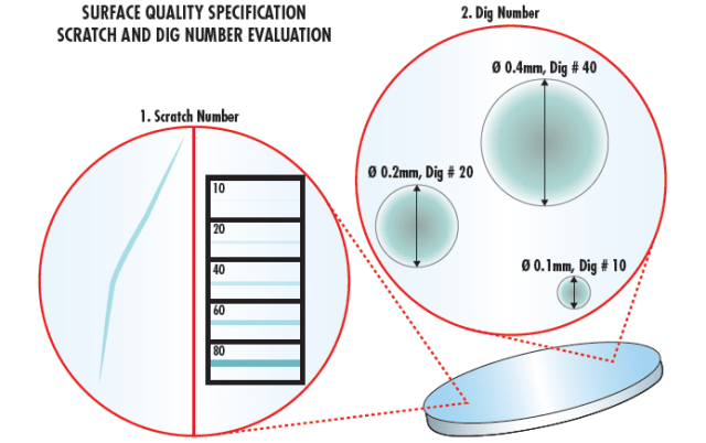
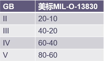
This standard is the United States military standard, which mainly describes the general technical conditions for the manufacture, assembly and inspection of fire control instruments and optical parts in detail. Most of the export parts have adopted this inspection standard for acceptance, and it is still in use today. In this standard, two sets of numbers are used to indicate the size of surface defects (defects). For example, 40/20 (or 40-20) limits scratch size while the latter limits pitting size. Road, bright road are called scratches. Spots, pits, and dots are called pitts. It is specified that the aspect ratio greater than 4:1 is a scratch, and that is less than 4:1 is a pitting. In the actual test, the scratch can be compared with the standard template, the standard sample has 10#, 20#, 40#, 60#, 80# 5 levels, the pitting point is measurable, the pitting point is 1/100mm as a unit of measurement, that is, the size of the pitting point is determined, 50# pitting point is the diameter D=0.5mm pitting point. The surface defect grade of a part is composed of two sets of numbers: scratch and pitting. MIL-O-13830B United States Military Standard and GB/T 1185-74 Surface Defects in Optical Parts can also be found in certain conditions for conversion between internal quality control and foreign trade sales.
GB/T 1185-2006
This standard is the current domestic standard, which has been greatly modified on the basis of the 74th edition. During the period, there was a transition version: GB/T 1185-1989 "Optical parts Surface Defects", from this version, the evaluation of defects has changed greatly. The current national standard has been used by more factories. Due to its corresponding to ISO 10110-7 "Optics and optical instruments Part 7 Surface Defects tolerance" and ISO 14997 "Optics and optical instrument parts Surface defects test methods", its evaluation and detection methods have gradually become international common, but it is not equivalent to the ISO standard. In this standard, the symbol of surface defects in optical mapping is: B/G×J, where B represents the defect code, G is the allowable number of surface defects, J is the series, characterizing the size of the defect, and is the square root of the area of the defect. M=J*J surface defect area as shown in the following figure, including general defect tolerance, coating layer defect tolerance, long scratch tolerance, broken edge tolerance: indicates that the basic level of general defect tolerance before coating is 0.63mm, the allowable number is 3; The basic grade of coating layer fault tolerance is 1.6mm, and the allowable number is

2. The basic series of long scratches is 0.1mm, and the allowable number is 2; The broken edge tolerance is 1mm. This standard is a relatively more quantitative method than MIL-O-13830B, which determines surface quality based on the physical size and frequency of surface defects on a given part area, but this method is relatively more time-consuming and expensive to detect.
Surface accurcay can simply be understood as referring to the flatness of the filter surface. It is like paving a road with cement or asphalt. A good road surface is smooth and smooth, and the car passes smoothly and quickly. If the paving is not good, the road surface ups and downs, potholes, the car can feel a very obvious sense of turbulence.
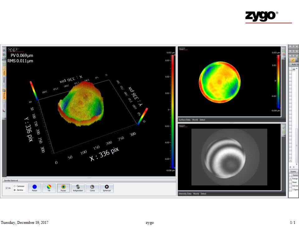
Surface accuracy refers to the deviation of the surface geometry of the optical element from the ideal shape. This deviation is generally quantified by a variety of parameters such as aperture number, local aperture number, PV, RMS, etc. Before figuring out the relationship between them, let's briefly understand the definition: the two parameters of aperture number (N) and local aperture appear more frequently in regular and complete optical drawings. Generally, it is mainly for the requirements of parts before processing. After processing, it is detected by interferometer and displayed with PV and RMS values. The PV value (Peak-to-Valley) is the height difference between the highest and lowest point of a surface. The RMS value (Root Mean Square) is the average of the data points in the detection area. In general, the PV value is 6-8 times the RMS value. So how to understand the relationship between aperture and PV? Simply remember: aperture is good, PV must be good. PV good, aperture is not necessarily good. Because PV is the relative value of the peak and trough of the aperture, the influence of local error is not considered. However, the influence of local aperture error should be considered when saying aperture.
The 3D model measured with the interferometer is generated by sampling data points, which visually and intuitively shows the convex and convex of the surface, which is helpful for the result evaluation. The interference fringe diagram provides detailed information about the surface topography, including the surface microstructure and interference phenomena.
Surface profile inspection of optical components is a complex and critical process that involves the integrated application of multiple parameters and techniques to ensure the performance and reliability of optical systems .
